Download Predictive Technology Model for Robust Nanoelectronic Design by Yu Cao (auth.) PDF

By Yu Cao (auth.)
Predictive know-how version for powerful Nanoelectronic layout explains a number of the technical mysteries at the back of the Predictive know-how version (PTM) that has been followed around the world in explorative layout examine. via actual derivation and know-how extrapolation, PTM is the de-factor machine version utilized in digital layout. This paintings explains the systematic version improvement and offers a consultant to powerful layout perform within the presence of variability and reliability concerns. Having interacted with a number of best semiconductor businesses and college examine groups, the writer brings a cutting-edge viewpoint on expertise scaling to this paintings and stocks insights won within the practices of machine modeling.
Read or Download Predictive Technology Model for Robust Nanoelectronic Design PDF
Similar technology books

Humans 3.0: The Upgrading of the Species
Existence for early people wasn't effortless. they could were in a position to stroll on ft and create instruments four million years in the past, yet they couldn't have in mind or speak. thankfully, humans obtained smarter, and issues acquired greater. They remembered on-the-spot recommendations and shared the dear details in their reports.

Central American Wars 1959 - 89
Considering that Fidel Castro's victory in Cuba in January 1959 the us were involved that any switch of presidency in a imperative American kingdom aren't herald an identical Soviet-backed communist regime; and to avoid this it has built more than a few responses, from direct army intervention, via help of neighborhood armies, to diplomatic isolation and fiscal blockade.
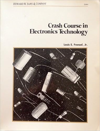
Crash course in electronics technology
Mixed with the 2 different Crash direction books, electronic know-how and Microprocessor know-how, this ebook kinds a whole direction in electronics and microcomputer know-how applicable for technical colleges, commercial education, and hobbyists. Crash direction in Electronics know-how teaches the fundamentals of electronics, parts, and circuits in an easy-to-understand layout.
- Introduction to Arduino: A piece of cake
- Building Knowledge Regions in North America: Emerging Technology Innovation Poles
- Chemistry of Nanocarbons
- Foldable Flex and Thinned Silicon Multichip Packaging Technology
- The used car buyer’s manual: how to find the best buy on a used car
- Space Tethers and Space Elevators
Additional resources for Predictive Technology Model for Robust Nanoelectronic Design
Example text
16). This circuit model 38 3 Predictive Technology Model of Enhanced CMOS Devices consists of two fully depleted SOI devices for the front and back transistors, respectively. , SPICE) [36]. 16 illustrates the detailed schematics of this equivalent circuit model. Two single gate transistors are used to capture the current conduction controlled by the front and back gate in a FinFET transistor. Each sub-transistor has its own definitions of gate voltage (VG), Vth, and Tox. Their sources and drains are electrically connected to form a four-node circuit.
Fossum, “Comparison of threshold-voltage shifts for uniaxial and biaxial tensile-stressed n-MOSFETs,” TED, vol. 25, no. 11, pp. 731–733, 2004. 9. H. 07) Immersion Lithography with Hybrid Dual-Damascene Structure and Porous Low-k BEOL,” in IEDM, pp. 685–688, 2006. 10. H. , 2008. 11. G. , “Scalability of the Si1-xGex Source/Drain technology for the 45-nm technology node and beyond,” TED, vol. 53, no. 7, Jul. 2006. 12. M. V. H. Lin, X. D. M. Niknejad, and C. Hu, “Modeling advanced FET technology in a compact model,” IEEE Transactions on Electron Devices, vol.
14. Z. , “High performance and low power transistors integrated in 65 nm bulk CMOS technology,” in IEDM Tech. , 2004, pp. 661–664. 15. C. C. , “A 90-nm CMOS device technology with high-speed, general-purpose, and low-leakage transistors for system on chip applications,” IEDM Tech. , pp. 65–68, 2002. 16. V. , “High speed 45 nm gate length CMOSFETs integrated into a 90 nm bulk technology incorporating strain engineering,” IEDM Tech. , pp. 77–80, 2003. 17. -F. , “High performance 50 nm CMOS devices for microprocessor and embedded processor core applications,” IEDM Tech.